Best National Partner Co., Ltd. specializes in wafer processing services that are essential to semiconductor manufacturing.
Through customized processing optimized for each customer’s production line, we help achieve both higher process efficiency and improved quality.
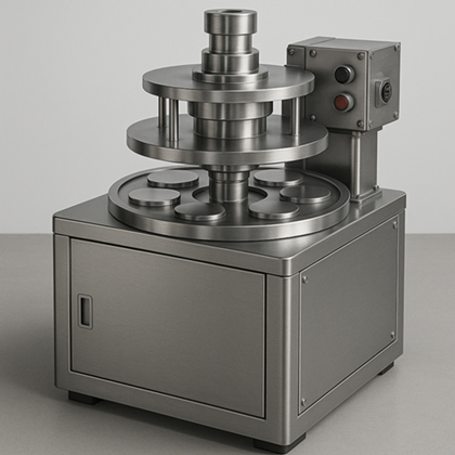
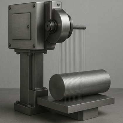
Major Wafer Processing Services
- -
- Polishing : High-planarization and ultra-fine surface processing
- -
- Thermal Oxidation : Formation of insulating oxide layers and compatibility with post-process steps
(PE-TEOS / LPCVD (SiN) / PE-CVD (SiO₂) / PE-CVD (SiN) wafers)
- -
- Back Grinding : Wafer thinning processes
- -
- Customized wafer thickness, from ultra-thin to thick wafers
- -
- Dicing : High-precision wafer cutting processes
- -
- Test & Reclaimed Wafer Supply : Cost-effective solutions for process testing and yield optimization
Customized Processing Support
- -
- Engineering support and specification adjustments tailored to customer products and production processes
- -
- Flexible manufacturing system capable of handling small-lot, multi-product orders as well as high-volume mass production
With our total wafer processing solutions, BNP empowers customers to enhance both productivity and quality assurance.